The Rise of ASML's AI Stack: How Veldhoven's Monopoly Is Being Modernised
ASML's High-NA EUV machines are the single most consequential bottleneck in global AI chip production. Inside Veldhoven, a parallel transformation is under way: the Dutch lithography giant is remaking its own engineering and manufacturing operations with AI, even as Dutch export-control policy tightens around its most powerful systems.
ASML's High-NA EUV lithography system is the one piece of industrial hardware that no nation, chipmaker, or hyperscaler can route around if it wants to manufacture leading-edge AI silicon at scale. That position - absolute, structural, and increasingly weaponised by geopolitics - makes what happens inside ASML's Veldhoven headquarters one of the most consequential engineering stories in European industry today.
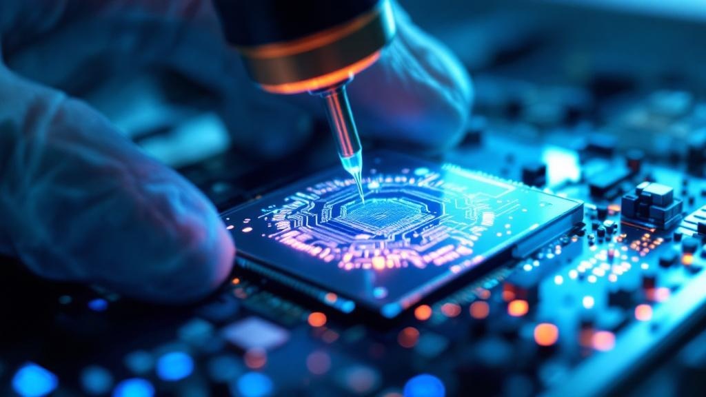
The company shipped its first High-NA EUV tool, the EXE:5000, to Intel's Hillsboro facility in late 2023, with further units destined for TSMC and Samsung thereafter. Each machine weighs roughly 150 tonnes, costs in excess of 350 million euros, and contains components sourced from more than 5,000 suppliers across Europe and beyond. Building and calibrating one is, by any reasonable measure, a feat of applied physics that requires predictive intelligence at every stage. That is precisely why ASML's internal AI programme is no longer a skunkworks experiment: it is now load-bearing infrastructure for the company's ability to deliver at all.
Advertisement
"Each High-NA EUV scanner weighs roughly 150 tonnes, costs in excess of 350 million euros, and contains components from more than 5,000 suppliers. Building and calibrating one requires predictive intelligence at every stage."
AI in Europe editorial analysis
Computational Lithography: Where AI Earns Its Keep First
The most technically mature application of AI inside ASML is computational lithography, the process of calculating how light behaves as it interacts with masks, lenses, and resist materials to print patterns at the two-nanometre node and below. Traditional optical proximity correction models are deterministic and slow; running a full-chip simulation for a High-NA exposure can take hundreds of CPU-hours on classical solvers.
ASML's software division has been replacing portions of that pipeline with neural-network-based surrogate models that approximate the physics at a fraction of the compute cost. The company's computational lithography platform, developed in part through its 2016 acquisition of HMI and its closer collaboration with Brion Technologies - a subsidiary absorbed into ASML's software stack - uses machine learning to compress simulation cycles. According to ASML's own technical publications and presentations at SPIE Advanced Lithography, the goal is not to replace physical models but to accelerate their execution so that chipmakers running EUV scanners can iterate on process recipes faster.
This matters operationally because High-NA's 0.55 numerical aperture introduces new aberration signatures and stochastic effects that did not exist at lower-NA. Training neural surrogate models on measured scanner data allows the software to adapt predictions to specific tool instances rather than relying on idealised simulations. TSMC and Samsung, both disclosed ASML customers for EUV systems, benefit directly: faster computational lithography cycles translate into shorter process development timelines for their most advanced nodes.
Predictive Maintenance: Keeping a 350-Million-Euro Machine Alive
A High-NA EUV scanner is not a machine that tolerates unplanned downtime gracefully. When one stops, it potentially halts the wafer flow for an entire advanced node programme. ASML has consequently invested heavily in what it calls its Customer Support programme, which includes a remote diagnostics and predictive maintenance layer that ingests telemetry from installed scanners in real time.
The system, described in ASML's 2023 and 2024 annual reports under the heading of service and installed-base management, uses anomaly detection models trained on sensor streams - laser power, alignment readings, reticle stage position, vacuum pressures - to flag degradation before it becomes failure. ASML employs roughly 7,000 service engineers globally; the AI layer is intended to make their interventions surgical rather than reactive.
The broader ambition, as outlined by ASML's executive team in investor presentations, is to increase scanner availability, measured in terms of uptime percentage, as a competitive differentiator in the service contract business. That business generated approximately 5.9 billion euros in service revenue in 2023 alone, representing a growing share of total income as the installed base expands. Predictive maintenance AI is, in other words, directly tied to a revenue line, which is why it receives serious engineering resource rather than being treated as a research curiosity.
Defect Classification and the Yield Problem
Beyond the scanner itself, ASML is deeply involved in the inspection and metrology layer that tells chipmakers whether a printed wafer meets specification. Through its e-beam inspection tools and its partnership with Zeiss - the German optics giant that supplies critical lens assemblies for EUV systems and operates as a formal technology partner - ASML has access to enormous volumes of defect imagery.
Defect classification using convolutional neural networks has become standard practice in semiconductor manufacturing, but the challenge at High-NA nodes is that defect morphologies are new, the signal-to-noise ratio in inspection images is worse at smaller feature sizes, and the ground-truth labelling required to train classifiers is expensive. ASML's approach, described in technical papers submitted to IEEE conferences, involves active learning pipelines that route ambiguous defect candidates to human reviewers, feeding confirmed labels back into the model continuously. The result is a classifier that improves as more High-NA wafers are processed, which gives early adopters such as Intel a compounding data advantage.
Imec, the Belgian semiconductor research institute based in Leuven, has been a critical partner in validating these defect classification workflows. As a pre-production test site for EUV and High-NA processes, Imec generates defect datasets under controlled conditions that ASML and its chipmaker customers use to benchmark their inspection AI before committing to volume production recipes.
The scale of ASML's business and the strategic stakes around its most advanced systems are best understood through the figures that underpin them: revenue concentrations, export exposure, and the engineering investment that makes it all function.
Export Controls: The Dutch Government Tightens Its Grip
ASML's internal AI modernisation is taking place against a backdrop of escalating state intervention in what the company can sell and to whom. The Dutch government, under pressure from the United States since at least 2019, has incrementally restricted export licences for ASML's most capable systems. The current Dutch coalition, led by the PVV and its coalition partners after the November 2023 election, has not reversed any of those restrictions and has indicated it views semiconductor export controls as a matter of national and allied security rather than purely commercial policy.
The Ministry of Economic Affairs and Climate Policy in The Hague administers the Dutch dual-use export licensing regime. ASML is required to apply for export licences for shipments of EUV and, now, DUV systems to certain destinations. China, which was ASML's third-largest market before restrictions tightened, has been progressively cut off from the most advanced DUV systems following Dutch government decisions in 2023, taken in coordination with the United States and Japan under the trilateral agreement first reported by Reuters in January 2023.
High-NA EUV has never been licenced for export to China at all. The Dutch government's position, confirmed in parliamentary briefings, is that High-NA constitutes a capability so far beyond anything currently in production elsewhere that granting export licences would be inconsistent with allied technology security commitments. ASML has not publicly contested that position, though it has consistently noted in shareholder communications that the lost China revenue creates a drag on near-term growth projections.
What the export control regime does, inadvertently but consequentially, is reinforce ASML's leverage over its Western customers. If TSMC, Intel, and Samsung are the only entities permitted to operate High-NA EUV tools, they become simultaneously ASML's most valuable customers and the nodes through which all leading-edge AI chip production must flow. The AI accelerators inside every major data centre - from Nvidia's Blackwell architecture to AMD's MI300 series - depend on wafers printed on ASML machines that no competitor can supply.
Where the Internal AI Programme Goes Next
ASML's chief technology officer, Martin van den Brink, who retired at the end of 2024 after decades defining the company's technical roadmap, consistently described the relationship between AI and lithography as symbiotic rather than one-directional. AI chips need better lithography; better lithography needs AI to design and operate. His successor, Christophe Fouquet, who became chief executive in April 2024, has signalled that the software and AI layer of ASML's business will be given greater strategic prominence.
That means the computational lithography, predictive maintenance, and defect classification programmes described above are likely to be centralised into a more coherent platform product rather than remaining as loosely connected internal tools. ASML has begun recruiting machine learning engineers and data scientists in Veldhoven and in its San Jose and Wilton offices at a rate that was not visible in its headcount data even three years ago.
The ambition, as far as it can be read from public statements and annual report language, is to make the AI stack a billable service rather than purely an operational cost centre. If ASML can sell computational lithography AI as a subscription alongside scanner hardware, it diversifies its revenue model and deepens customer lock-in simultaneously. For a company whose hardware monopoly is already the subject of intense geopolitical attention, extending that monopoly into software and AI would be a logical, if politically sensitive, next move.
THE AI IN EUROPE VIEW
ASML's monopoly position is one of Europe's few genuine structural advantages in the global technology competition, and the company deserves credit for investing seriously in the AI that makes its machines manufacturable and serviceable at scale. Computational lithography acceleration, predictive maintenance, and defect classification are not marketing categories: they are the engineering work that keeps the world's most complex industrial systems running. Europe should be building on this.
But two things ought to make policymakers and industry observers uncomfortable. First, the export control regime, however necessary, is being designed in Washington and then adopted in The Hague. The Dutch Ministry of Economic Affairs is administering a policy whose strategic logic was written elsewhere. That is a sovereignty problem dressed up as an alliance benefit, and the Netherlands should be pushing harder for a formal European framework rather than operating as a bilateral instrument of American technology policy.
Second, if ASML succeeds in turning its AI stack into a software subscription layer sold alongside hardware, it will have created a second monopoly nested inside the first. That is commercially brilliant and competitively concerning in equal measure. European competition regulators should be watching now, before the market structure is set.
Updates
published_at reshuffled 2026-04-29 to spread distribution per editorial directive
Byline migrated from "Eva Janssen" (eva-janssen) to Intelligence Desk per editorial integrity policy.
AI Terms in This Article6 terms
machine learning
Software that improves at tasks by learning from data rather than being explicitly programmed.
benchmark
A standardized test used to compare AI model performance.
at scale
Applied broadly, to a large number of users or use cases.
leverage
Use effectively.
alignment
Ensuring AI systems pursue goals that match human intentions and values.
dual-use
Technology that can be applied for both civilian and military purposes.
Advertisement
Comments
Sign in to join the conversation. Be civil, be specific, link your sources.


Comments
Sign in to join the conversation. Be civil, be specific, link your sources.